Circuit Board / PCB
Circuit board PCB interface. Ideal for landing pages, saas. AI-ready template.
Use case: Landing pages, SaaS
Historical Context
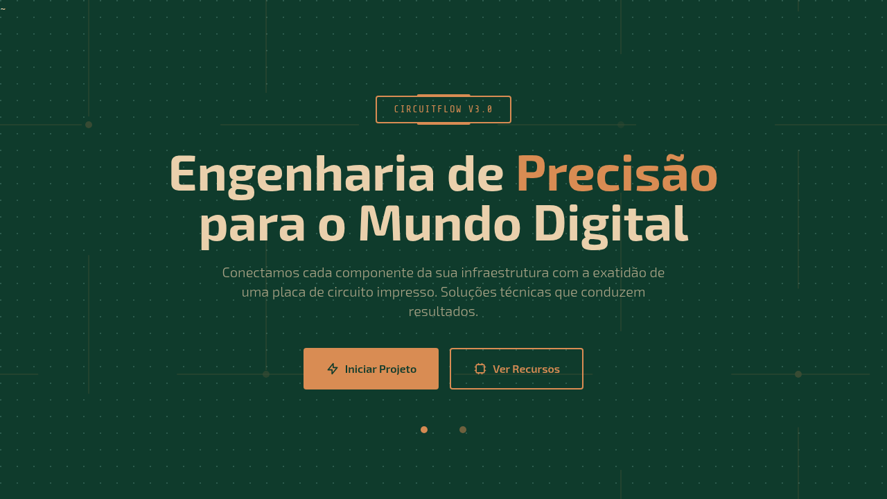
Circuit boards were never meant to be beautiful. They were engineered — routed by necessity, constrained by physics. Copper traces follow the shortest viable path between components. Solder pads exist at precise intervals dictated by pin spacing. Every line serves a function. And yet, somewhere in the late '80s, designers started lifting these patterns out of their enclosures and plastering them across posters, album covers, and tech branding. The PCB became shorthand for 'this is the future.' It makes sense if you think about it. A circuit board is an engineering drawing that actually works. It's a blueprint that conducts electricity. There's something deeply satisfying about that overlap — form following function so literally that the function becomes the form. The green soldermask, the gold traces, the repetitive geometry of vias marching across a substrate. It reads as complexity, as intelligence, as something built with intention. The aesthetic peaked in the '90s cyberpunk era but never really left. It just got more refined. Today's PCB-inspired patterns strip away the literal green-and-gold and keep the topology — the branching paths, the nodes, the sense of interconnection. Less motherboard, more abstract network.
When to Use
Reach for PCB patterns when you need to signal technical depth without resorting to generic binary code or floating hologram clichés. They work beautifully for hardware startups, IoT product pages, electronics brands, and tech education platforms where the audience actually knows what a trace route looks like. Also strong for developer tools and embedded systems companies. Avoid if your product has zero hardware connection — borrowed credibility reads as costume.
Design Principles
- Maintain trace logic — lines should connect to nodes, not float randomly. Even abstracted, the topology needs to feel routable.
- Respect the grid. Real PCBs snap to manufacturing grids. Your pattern should too. Irregular organic curves break the illusion instantly.
- Use restraint with color. Monochrome or duotone reads sophisticated. Full-color rainbow traces look like a toy store flyer from 2003.
- Scale matters — zoomed-in traces at macro scale feel architectural and premium. Zoomed-out full-board views risk looking like clip art.
- Leave breathing room. Actual PCBs have ground planes — large empty copper areas. Your composition needs that same negative space to avoid visual noise.
DESIGN.md
---
version: "alpha"
name: "Circuit Board / PCB"
description: "Circuit board PCB interface. Ideal for landing pages, saas. AI-ready template."
colors:
  primary: "#0F3B2C"
  secondary: "#D98C53"
  tertiary: "#EAD0AC"
  neutral: "#2D5C4E"
  surface: "#8B7355"
  accent: "#C17817"
typography:
  h1:
    fontFamily: System UI stack
    fontSize: 2.25rem
    fontWeight: 700
  body-md:
    fontFamily: System UI stack
    fontSize: 1rem
    fontWeight: 400
  label-caps:
    fontFamily: System UI stack
    fontSize: 0.75rem
    fontWeight: 500
components:
  button-primary:
    backgroundColor: "{colors.primary}"
    textColor: "{colors.neutral}"
    padding: 12px
---

## Overview

Circuit board PCB interface. Ideal for landing pages, saas. AI-ready template. Circuit boards were never meant to be beautiful. They were engineered — routed by necessity, constrained by physics. Copper traces follow the shortest viable path between components. Solder pads exist at precise intervals dictated by pin spacing. Every line serves a function. And yet, somewhere in the late '80s, designers started lifting these patterns out of their enclosures and plastering them across posters, album covers, and tech branding. The PCB became shorthand for 'this is the future.'

It makes sense if you think about it. A circuit board is an engineering drawing that actually works. It's a blueprint that conducts electricity. There's something deeply satisfying about that overlap — form following function so literally that the function becomes the form. The green soldermask, the gold traces, the repetitive geometry of vias marching across a substrate. It reads as complexity, as intelligence, as something built with intention.

The aesthetic peaked in the '90s cyberpunk era but never really left. It just got more refined. Today's PCB-inspired patterns strip away the literal green-and-gold and keep the topology — the branching paths, the nodes, the sense of interconnection. Less motherboard, more abstract network.

- Density: 7/10 — Compact
- Variance: 2/10 — Structured
- Motion: 6/10 — Expressive

- **Style:** Technical, Electronic, Structured, Precise
- **Keywords:** Printed circuit board, copper traces, solder pads, IC chip outlines, electronic schematic, precision-engineered, technical, network-based
- **Era:** Technical Electronic
- **Light/Dark:** ✓ Full / ✓ Full

## Colors

- **PCB Green** (#0F3B2C) — Primary surface or dominant color
- **Copper Trace** (#D98C53) — Metallic accent, decorative detail
- **Cream Label** (#EAD0AC) — Light surface, card backgrounds
- **Dark Green** (#2D5C4E) — Dark surface, primary background
- **Warm Brown** (#8B7355) — Extended palette, decorative use
- **Gold Pin** (#C17817) — Premium accent, decorative highlights


## Typography

- **Display / Hero:** System UI stack (-apple-system, sans-serif) — Weight 700, tight tracking, used for headline impact
- **Body:** System UI stack (-apple-system, sans-serif) — Weight 400, 16px/1.6 line-height, max 72ch per line
- **UI Labels / Captions:** System UI stack (-apple-system, sans-serif) — 0.875rem, weight 500, slight letter-spacing
- **Monospace:** JetBrains Mono — Used for code, metadata, and technical values

Scale:
- Hero: clamp(2.5rem, 5vw, 4rem)
- H1: 2.25rem
- H2: 1.5rem
- Body: 1rem / 1.6
- Small: 0.875rem


## Layout

- **Grid:** CSS Grid primary. Max-width containment: 1280px centered with 1.5rem side padding.
- **Spacing rhythm:** Balanced. Base unit: 0.5rem (8px).
- **Section vertical gaps:** clamp(4rem, 8vw, 8rem).
- **Hero layout:** Split-screen (text left, visual right).
- **Feature sections:** Zig-zag alternating text+image rows. No 3-equal-columns.
- **Mobile collapse:** All multi-column layouts collapse below 768px. No horizontal overflow.
- **z-index contract:** base (0) / sticky-nav (100) / overlay (200) / modal (300) / toast (500).


## Elevation & Depth

Flat technical illustration, trace drawing animations (stroke-dasharray), signal pulse along traces, component highlight on hover, data flow visualization

- **Physics:** Spring — stiffness 120, damping 20. Confident, weighted transitions.
- **Entry animations:** Fade + translate-Y (16px → 0) over 480ms ease-out. Staggered cascades for lists: 100ms between items.
- **Hover states:** Scale(1.03) + shadow lift over 200ms.
- **Page transitions:** Fade + slide (300ms).
- **Performance:** Only transform and opacity animated. No layout-triggering properties.


## Shapes

Base corner radius: 8px. See rounded tokens in front matter for the full scale.


## Components

- **Primary Button:** Subtly rounded (0.5rem) shape. Accent color fill. Hover: 8% darken + subtle lift shadow. Active: -1px translate tactile press. Font weight 600. No outer glows.
- **Secondary / Ghost Button:** Outline variant. 1.5px border in muted color. Text in primary color. Hover: subtle background fill.
- **Cards:** Subtly rounded (0.5rem) corners. Surface background. Subtle shadow (0 2px 12px rgba(0,0,0,0.06)). 1px border stroke.
- **Inputs:** Label above input. 1px border stroke. Focus ring: 2px accent color offset 2px. Error text below in semantic red. No floating labels.
- **Navigation:** Primary surface background. Active item: accent color indicator. Font weight 500 when active.
- **Skeletons:** Shimmer animation matching component dimensions. No circular spinners.
- **Empty States:** Icon-based composition with descriptive text and action button.


## Do's and Don'ts

- No emojis in UI — use icon system only (Lucide, Heroicons)
- No pure black (#000000) — use off-black or charcoal variants
- No oversaturated accent colors (saturation cap: 80%)
- No 3-column equal-width feature layouts — use zig-zag or asymmetric grid
- No `h-screen` — use `min-h-[100dvh]`
- No AI copywriting clichés: "Elevate", "Seamless", "Unleash", "Next-Gen"
- No broken external image links — use picsum.photos or inline SVG
- No generic lorem ipsum in demos

- Do PCB green background
- Do Copper traces visible
- Do Solder pad nodes
- Do IC chip outlines
- Do Network layout
- Do Technical precision


## Use Case

Landing pages, SaaS
Technical Specs
CSS
background: #0F3B2C, color: #EAD0AC, border: copper-colored traces, SVG paths for circuit lines, stroke-dasharray for trace animation, circular nodes for solder pads, monospace font for labels
Variables
--pcb-green: #0F3B2C, --copper-trace: #D98C53, --cream-label: #EAD0AC, --dark-green: #2D5C4E, --trace-width: 2px, --pad-radius: 6px
Checklist
☐ PCB green background, ☐ Copper traces visible, ☐ Solder pad nodes, ☐ IC chip outlines, ☐ Network layout, ☐ Technical precision
Colors
Primary
Secondary
Effects
Flat technical illustration, trace drawing animations (stroke-dasharray), signal pulse along traces, component highlight on hover, data flow visualization
Light/Dark
✓ Full / ✓ Full
AI Prompt
Act as a Senior Frontend Engineer and Expert UI Designer.
Your task is to code a complete Landing Page on the first attempt.
- Landing Page Theme: <INSERT THEME>
- Sections to add: <INSERT SECTIONS>

Generate the final code immediately following these definitions:

## Style

- **Name:** Circuit Board / PCB
- **Type:** Technical, Electronic, Structured, Precise
- **Keywords:** Printed circuit board, copper traces, solder pads, IC chip outlines, electronic schematic, precision-engineered, technical, network-based
- **Era:** Technical Electronic
- **Light/Dark:** ✓ Full / ✓ Full

## Color Palette

- **Primary:** PCB Green #0F3B2C, Copper Trace #D98C53, Cream Label #EAD0AC, Dark Green #2D5C4E
- **Secondary:** Warm Brown #8B7355, Gold Pin #C17817, solder silver, matte FR-4 substrate

## Visual Effects

Flat technical illustration, trace drawing animations (stroke-dasharray), signal pulse along traces, component highlight on hover, data flow visualization

## AI Visual Direction

Design a circuit board PCB interface. Use: PCB green background (#0F3B2C), copper trace lines connecting elements, solder pad nodes, IC chip outlines, electronic schematic aesthetic, network-based layout, technical precision, FR-4 substrate texture.

## CSS Technical

```css
background: #0F3B2C, color: #EAD0AC, border: copper-colored traces, SVG paths for circuit lines, stroke-dasharray for trace animation, circular nodes for solder pads, monospace font for labels
```

## Design System Variables

```css
--pcb-green: #0F3B2C, --copper-trace: #D98C53, --cream-label: #EAD0AC, --dark-green: #2D5C4E, --trace-width: 2px, --pad-radius: 6px
```

## Implementation Checklist

- ☐ PCB green background
- ☐ Copper traces visible
- ☐ Solder pad nodes
- ☐ IC chip outlines
- ☐ Network layout
- ☐ Technical precision

## Execution Rules

1. Strictly follow the defined visual style.
2. Use high-quality inline SVG icons (Heroicons or Lucide style) — NEVER use emojis as icons.
3. Add `cursor-pointer` and smooth `hover` states (transition-all) on all interactive elements.
4. Required Page Structure:
   - Navbar (Logo + Links + CTA)
   - Hero Section (Impactful Headline + Subtitle + 2 buttons + 3D/Abstract visual element via CSS)
   - Features (3 cards with icons)
   - Testimonials (3 cards)
   - Pricing (3 tiers, highlight the middle one)
   - Final CTA
   - Full Footer with social links, privacy policy, terms of use, contact and SEO links.
5. All text content must be in English.
6. The visual must be CLEARLY distinct — do not create a "default Bootstrap" design. Force the use of the provided design system variables.
7. Use `<style>` tags in the head for custom classes (especially for complex backdrop-filter effects and animations) that Tailwind CDN doesn't cover.
8. Full Responsiveness: Layout must adapt perfectly to Mobile, Tablet and Desktop (vertical stack on mobile).
9. Include basic SEO, Viewport and Open Graph meta tags in `<head>`.
10. Footer must contain: Copyright 2026, Secondary navigation links and Social media icons.
11. Make the creative decisions needed to deliver the complete, functional result now.
Related
Last synced: 4/1/2026