Estilo de Litografia de Precisão
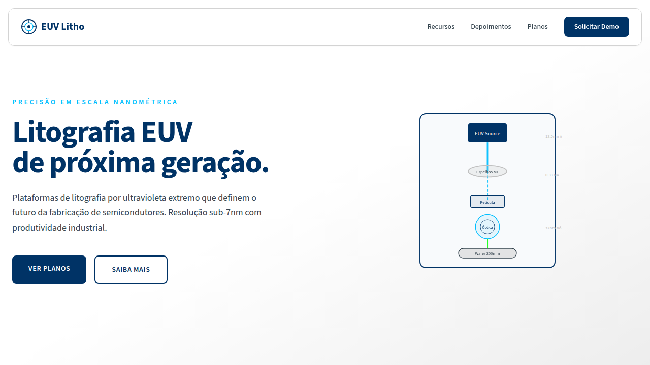
Precise and industrial landing page for EUV technology. Ideal for landing pages, modern websites. AI-ready template.
Use case: Landing pages, Modern websites
Historical Context
There's something almost spiritual about EUV lithography. You're projecting light at 13.5 nanometers — a wavelength so short it gets absorbed by air itself — onto silicon wafers to etch patterns smaller than a virus. The entire process happens in a vacuum, bouncing off multilayer mirrors with tolerances measured in atoms. That's not engineering. That's obsession made physical. The visual language born from this world is unmistakable. Stacked translucent layers. Repeating geometric patterns at impossible density. Color palettes pulled from thin-film interference — those iridescent blues and violets you see when light diffracts off a wafer's surface. Everything is grid-locked, everything registers perfectly to what came before it. Designers working in deep tech have been borrowing this vocabulary for years, but rarely with the rigor it deserves. The best implementations treat the screen like a reticle — every element placed with nanometer intent, every layer serving a structural purpose. No decoration. Pure function rendered beautiful through sheer precision.
When to Use
Reach for this when your audience understands tolerances. Chip manufacturers, photonics companies, semiconductor equipment makers, quantum computing startups — anyone whose product exists at the boundary of what's physically possible. It works for scientific visualization dashboards, deep tech investor decks, and hardware company brand systems. Skip it for consumer products. This style rewards attention and punishes skimming. If your users won't slow down to read a datasheet, they won't appreciate lithographic precision in your interface either.
Design Principles
- Layer registration — Every visual layer must align to a shared coordinate system, just as each lithography pass registers to fiducial marks on the wafer. Misalignment is immediately visible and always wrong.
- Nanoscale density — Pack information tight. Use repeating micro-patterns, dense grids, and fine linework that rewards closer inspection. Whitespace exists for optical function, not aesthetic comfort.
- Thin-film color — Derive palette from interference patterns: spectral violets, deep UV blues, wafer-gold, silicon grey. Colors shift subtly with context, never shout.
- Vacuum clarity — Remove atmospheric noise. No gradients mimicking depth, no soft shadows, no blur. Every edge is hard-cut, every boundary defined with the precision of a photomask.
- Process hierarchy — Structure information like lithography steps: base layer first, each subsequent pass adding finer detail. The user should feel the build-up from substrate to finished circuit.
DESIGN.md
---
version: "alpha"
name: "Estilo de Litografia de Precisão"
description: "Precise and industrial landing page for EUV technology. Ideal for landing pages, modern websites. AI-ready template."
colors:
  primary: "#003366"
  secondary: "#C0C0C0"
  tertiary: "#FFFFFF"
  neutral: "#36454F"
  surface: "#00BFFF"
  accent: "#00FF00"
typography:
  h1:
    fontFamily: Source Sans Pro
    fontSize: 2.5rem
    fontWeight: 700
  body-md:
    fontFamily: Source Sans Pro
    fontSize: 1rem
    fontWeight: 400
components:
  button-primary:
    backgroundColor: "{colors.primary}"
    textColor: "{colors.neutral}"
    padding: 12px
---

## Overview

Precise and industrial landing page for EUV technology. Ideal for landing pages, modern websites. AI-ready template. There's something almost spiritual about EUV lithography. You're projecting light at 13.5 nanometers — a wavelength so short it gets absorbed by air itself — onto silicon wafers to etch patterns smaller than a virus. The entire process happens in a vacuum, bouncing off multilayer mirrors with tolerances measured in atoms. That's not engineering. That's obsession made physical.

The visual language born from this world is unmistakable. Stacked translucent layers. Repeating geometric patterns at impossible density. Color palettes pulled from thin-film interference — those iridescent blues and violets you see when light diffracts off a wafer's surface. Everything is grid-locked, everything registers perfectly to what came before it.

Designers working in deep tech have been borrowing this vocabulary for years, but rarely with the rigor it deserves. The best implementations treat the screen like a reticle — every element placed with nanometer intent, every layer serving a structural purpose. No decoration. Pure function rendered beautiful through sheer precision.

- Density: 3/10 — Airy
- Variance: 2/10 — Structured
- Motion: 4/10 — Subtle

- **Style:** Industrial, Scientific, Precise
- **Keywords:** lithography, EUV, semiconductors, nanotechnology, precision, scientific, industrial, advanced, cleanroom, structured
- **Era:** 2026+ Microchip Revolution
- **Light/Dark:** ✓ Full / ✗ No

## Colors

- **Azul Científico** (#003366) — Accent highlight, links and focus states
- **Prata** (#C0C0C0) — Secondary surface or text color
- **Branco** (#FFFFFF) — Light surface, card backgrounds
- **Cinza Escuro** (#36454F) — Dark surface, primary background
- **Azul Elétrico** (#00BFFF) — Secondary accent
- **Verde** (#00FF00) — Success states, positive indicators
- **Laranja** (#FFA500) — Warm accent, call-to-action secondary
- **Cinza Claro** (#D3D3D3) — Secondary text, borders, muted elements


## Typography

- **Display / Hero:** Source Sans Pro — Weight 700, tight tracking, used for headline impact
- **Body:** Source Sans Pro — Weight 400, 16px/1.6 line-height, max 72ch per line
- **UI Labels / Captions:** Source Sans Pro — 0.875rem, weight 500, slight letter-spacing
- **Monospace:** JetBrains Mono — Used for code, metadata, and technical values

Scale:
- Hero: clamp(2.5rem, 5vw, 4rem)
- H1: 2.25rem
- H2: 1.5rem
- Body: 1rem / 1.6
- Small: 0.875rem


## Layout

- **Grid:** CSS Grid primary. Max-width containment: 1280px centered with 1.5rem side padding.
- **Spacing rhythm:** Balanced. Base unit: 0.5rem (8px).
- **Section vertical gaps:** clamp(4rem, 8vw, 8rem).
- **Hero layout:** Split-screen (text left, visual right).
- **Feature sections:** Zig-zag alternating text+image rows. No 3-equal-columns.
- **Mobile collapse:** All multi-column layouts collapse below 768px. No horizontal overflow.
- **z-index contract:** base (0) / sticky-nav (100) / overlay (200) / modal (300) / toast (500).


## Elevation & Depth

Visualizações de feixes de luz (EUV), diagramas de máquinas complexas, brilhos sutis em componentes de alta tecnologia, tipografia técnica e limpa, micro-interações de dados, elementos modulares, animações de processo de fabricação.

- **Physics:** Ease-out curves, 200-300ms duration. Smooth and predictable.
- **Entry animations:** Fade + translate-Y (16px → 0) over 420ms ease-out. Staggered cascades for lists: 80ms between items.
- **Hover states:** Subtle color shift + shadow adjustment over 200ms.
- **Page transitions:** Fade only (200ms).
- **Performance:** Only transform and opacity animated. No layout-triggering properties.


## Shapes

Base corner radius: 8px. See rounded tokens in front matter for the full scale.


## Components

- **Primary Button:** Subtly rounded (0.5rem) shape. Accent color fill. Hover: 8% darken + subtle lift shadow. Active: -1px translate tactile press. Font weight 600. No outer glows.
- **Secondary / Ghost Button:** Outline variant. 1.5px border in muted color. Text in primary color. Hover: subtle background fill.
- **Cards:** Subtly rounded (0.5rem) corners. Surface background. Subtle shadow (0 2px 12px rgba(0,0,0,0.06)). 1px border stroke.
- **Inputs:** Label above input. 1px border stroke. Focus ring: 2px accent color offset 2px. Error text below in semantic red. No floating labels.
- **Navigation:** Primary surface background. Active item: accent color indicator. Font weight 500 when active.
- **Skeletons:** Shimmer animation matching component dimensions. No circular spinners.
- **Empty States:** Icon-based composition with descriptive text and action button.


## Do's and Don'ts

- No emojis in UI — use icon system only (Lucide, Heroicons)
- No pure black (#000000) — use off-black or charcoal variants
- No oversaturated accent colors (saturation cap: 80%)
- No 3-column equal-width feature layouts — use zig-zag or asymmetric grid
- No `h-screen` — use `min-h-[100dvh]`
- No AI copywriting clichés: "Elevate", "Seamless", "Unleash", "Next-Gen"
- No broken external image links — use picsum.photos or inline SVG
- No generic lorem ipsum in demos

- Do Visualizações de feixes EUV
- Do Diagramas de máquinas
- Do Brilhos em componentes
- Do Tipografia técnica
- Do Micro-interações de dados
- Do Animações de processo.


## Use Case

Landing pages, Modern websites
Technical Specs
CSS
background: #FFFFFF, color: #003366, border-bottom: 1px solid #D3D3D3, box-shadow: 0 2px 5px rgba(0,0,0,0.05), font-family: "Source Sans Pro, sans-serif", transition: all 0.3s ease-in-out, background-image: linear-gradient(to bottom, #F8F8F8, #FFFFFF), .euv-beam-animation, .machine-diagram.
Variables
--scientific-blue: #003366, --silver: #C0C0C0, --white: #FFFFFF, --dark-grey: #36454F, --euv-glow: rgba(0,191,255,0.3), --font-scientific: "Source Sans Pro, sans-serif", --shadow-light: 0 2px 5px rgba(0,0,0,0.05).
Checklist
☐ Visualizações de feixes EUV, ☐ Diagramas de máquinas, ☐ Brilhos em componentes, ☐ Tipografia técnica, ☐ Micro-interações de dados, ☐ Animações de processo.
Colors
Primary
Secondary
Effects
Visualizações de feixes de luz (EUV), diagramas de máquinas complexas, brilhos sutis em componentes de alta tecnologia, tipografia técnica e limpa, micro-interações de dados, elementos modulares, animações de processo de fabricação.
Light/Dark
✓ Full / ✗ No
AI Prompt
Act as a Senior Frontend Engineer and Expert UI Designer.
Your task is to code a complete Landing Page on the first attempt.
- Landing Page Theme: <INSERT THEME>
- Sections to add: <INSERT SECTIONS>

Generate the final code immediately following these definitions:

## Style

- **Name:** Estilo de Litografia de Precisão
- **Type:** Industrial, Scientific, Precise
- **Keywords:** lithography, EUV, semiconductors, nanotechnology, precision, scientific, industrial, advanced, cleanroom, structured
- **Era:** 2026+ Microchip Revolution
- **Light/Dark:** ✓ Full / ✗ No

## Color Palette

- **Primary:** Azul Científico #003366, Prata #C0C0C0, Branco #FFFFFF, Cinza Escuro #36454F
- **Secondary:** Azul Elétrico #00BFFF, Verde #00FF00, Laranja #FFA500, Cinza Claro #D3D3D3

## Visual Effects

Visualizações de feixes de luz (EUV), diagramas de máquinas complexas, brilhos sutis em componentes de alta tecnologia, tipografia técnica e limpa, micro-interações de dados, elementos modulares, animações de processo de fabricação.

## AI Visual Direction

Design a precise and industrial landing page for EUV technology. Use: scientific blue and silver palette, EUV light beam visualizations, complex machine diagrams, subtle high-tech glows, clean technical typography, data micro-interactions, modular elements, manufacturing process animations, industrial and structured feel.

## CSS Technical

```css
background: #FFFFFF, color: #003366, border-bottom: 1px solid #D3D3D3, box-shadow: 0 2px 5px rgba(0,0,0,0.05), font-family: "Source Sans Pro, sans-serif", transition: all 0.3s ease-in-out, background-image: linear-gradient(to bottom, #F8F8F8, #FFFFFF), .euv-beam-animation, .machine-diagram.
```

## Design System Variables

```css
--scientific-blue: #003366, --silver: #C0C0C0, --white: #FFFFFF, --dark-grey: #36454F, --euv-glow: rgba(0,191,255,0.3), --font-scientific: "Source Sans Pro, sans-serif", --shadow-light: 0 2px 5px rgba(0,0,0,0.05).
```

## Implementation Checklist

- ☐ Visualizações de feixes EUV
- ☐ Diagramas de máquinas
- ☐ Brilhos em componentes
- ☐ Tipografia técnica
- ☐ Micro-interações de dados
- ☐ Animações de processo.

## Execution Rules

1. Strictly follow the defined visual style.
2. Use high-quality inline SVG icons (Heroicons or Lucide style) — NEVER use emojis as icons.
3. Add `cursor-pointer` and smooth `hover` states (transition-all) on all interactive elements.
4. Required Page Structure:
   - Navbar (Logo + Links + CTA)
   - Hero Section (Impactful Headline + Subtitle + 2 buttons + 3D/Abstract visual element via CSS)
   - Features (3 cards with icons)
   - Testimonials (3 cards)
   - Pricing (3 tiers, highlight the middle one)
   - Final CTA
   - Full Footer with social links, privacy policy, terms of use, contact and SEO links.
5. All text content must be in English.
6. The visual must be CLEARLY distinct — do not create a "default Bootstrap" design. Force the use of the provided design system variables.
7. Use `<style>` tags in the head for custom classes (especially for complex backdrop-filter effects and animations) that Tailwind CDN doesn't cover.
8. Full Responsiveness: Layout must adapt perfectly to Mobile, Tablet and Desktop (vertical stack on mobile).
9. Include basic SEO, Viewport and Open Graph meta tags in `<head>`.
10. Footer must contain: Copyright 2026, Secondary navigation links and Social media icons.
11. Make the creative decisions needed to deliver the complete, functional result now.
Related
Last synced: 4/1/2026